- 您现在的位置:买卖IC网 > PDF目录17110 > ATF15XX-DK3 (Atmel)KIT DEV FOR ATF15XX CPLD'S PDF资料下载
参数资料
| 型号: | ATF15XX-DK3 |
| 厂商: | Atmel |
| 文件页数: | 16/44页 |
| 文件大小: | 0K |
| 描述: | KIT DEV FOR ATF15XX CPLD'S |
| 产品培训模块: | MCU Product Line Introduction |
| 标准包装: | 1 |
| 系列: | Logic Doubling® |
| 类型: | CPLD |
| 适用于相关产品: | ATF15xx 系列 CPLD |
| 所含物品: | CPLD 编程器板,44-TQFP,插口适配器板,下载线缆,CD-ROM。 样品和用户指南 |
| 产品目录页面: | 609 (CN2011-ZH PDF) |
| 配用: | ATF15XXDK3-SAJ84-ND - ADAPTER SKT ATF15XXBE 84/84PLCC ATF15XXDK3-SAA100-ND - ADAPTER SKT ATF15XXB PLCC/TQFP ATF15XXDK3-SAJ44-ND - ADAPTER SKT ATF15XXBE 84/44PLCC |
| 相关产品: | ATF1504AS-7JX44-ND - IC CPLD 7NS HI PERFORM 44PLCC ATF1508AS-10AAI128-ND - IC CPLD 128MC 5.0V 128-LQFP ATF1504BE-7AU44-ND - IC CPLD 64MC 1.8V 44-TQFP ATF1504BE-7AU100-ND - IC CPLD 64MC 1.8V 100-TQFP ATF1504BE-5AX44-ND - IC CPLD 64MC 1.8V 44-TQFP ATF1504BE-5AX100-ND - IC CPLD 64MC 1.8V 100-TQFP ATF1502BE-5AX44-ND - IC CPLD 64MC 1.8V 44-TQFP ATF1504AS-10JU84-ND - IC CPLD 10NS 84PLCC ATF1504AS-10JU44-ND - IC CPLD 10NS 44PLCC ATF1508AS-7JX84-ND - IC CPLD 7NS 84PLCC 更多... |
第1页第2页第3页第4页第5页第6页第7页第8页第9页第10页第11页第12页第13页第14页第15页当前第16页第17页第18页第19页第20页第21页第22页第23页第24页第25页第26页第27页第28页第29页第30页第31页第32页第33页第34页第35页第36页第37页第38页第39页第40页第41页第42页第43页第44页
�� �
�
�Hardware� Description�
�shows� the� pin� numbers� of� the� GCLR� and� OE1� dedicated� input� pins� of� the� ATF15xx� in� all�
�the� different� available� package� types.�
�Figure� 2-5.� Circuit� Diagram� of� Push-button� Switches� and� Selectable� Jumpers� for�
�GCLR� and� OE1�
�Table� 2-13.� Pin� Numbers� of� GCLR� and� OE1�
�44-pin�
�TQFP�
�44-pin�
�PLCC�
�84-pin�
�PLCC�
�100-pin�
�TQFP�
�GCLR�
�OE1�
�39�
�38�
�1�
�44�
�1�
�84�
�89�
�88�
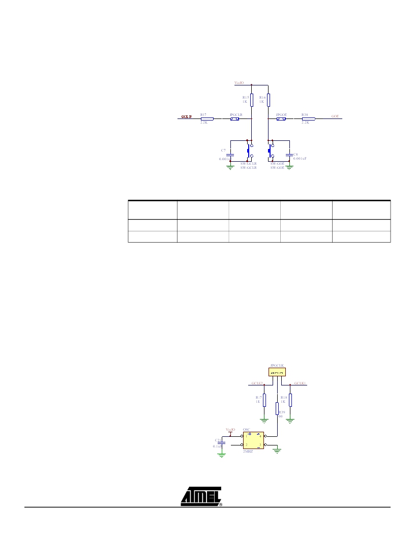
�2.1.5�
�2� MHz� Oscillator� and�
�Clock� Selection�
�Jumper�
�The� Clock� Selection� Jumper,� labeled� JP-GCLK,� on� the� CPLD� Development/Program-�
�mer� Board� is� a� two-position� jumper� that� allows� the� users� to� select� which� GCLK�
�dedicated� input� pin� (either� GCLK1� or� GCLK2)� of� the� ATF15xx� should� be� connected� to�
�the� output� of� the� 2� MHz� oscillator.� In� addition,� the� jumper� can� be� removed� to� allow� an�
�external� clock� source� to� be� connected� to� GCLK1� and/or� GCLK2� of� the� ATF15xx.� Figure�
�2-6� is� the� circuit� diagram� of� the� oscillator� and� selection� jumper.� Table� 2-14� on� page� 2-10�
�shows� the� pin� numbers� for� the� GCLK1� and� GCLK2� dedicated� input� pins� of� the� ATF15xx�
�in� all� the� different� available� package� types.�
�Note:�
�If� GCLK1� jumper� is� set,� the� jumper� will� be� located� toward� the� side� of� the� board.�
�On� the� other� hand,� if� GCLK2� jumper� is� set,� the� jumper� will� be� located� toward� the�
�middle� of� the� board.�
�Figure� 2-6.� Circuit� Diagram� of� Oscillator� and� Clock� Selection� Jumper�
�ATF15xx-DK3� Development� Kit� User� Guide�
�2-9�
�3605B–PLD–05/06�
�相关PDF资料 |
PDF描述 |
|---|---|
| ADR02WARZ-REEL7 | IC VREF SERIES PREC 5V 8-SOIC |
| EVAL-ADUC812QSZ | BOARD EVALUATION FOR ADUC812 |
| ECM30DCWD | CONN EDGECARD 60POS DIP .156 SLD |
| ADR03WARZ-R7 | IC VREF SERIES PREC 2.5V 8SOIC |
| SC43B-1R4 | INDUCTOR SMD 1.4UH 2.20A 7.96MHZ |
相关代理商/技术参数 |
参数描述 |
|---|---|
| ATF15XXDK3-SAA100 | 功能描述:插座和适配器 SOCKET ADAPTER RoHS:否 制造商:Silicon Labs 产品:Adapter 用于:EM35x |
| ATF15XXDK3-SAA128 | 功能描述:插座和适配器 128-pin LQFP Socket Adapter to F15XX-DK3 RoHS:否 制造商:Silicon Labs 产品:Adapter 用于:EM35x |
| ATF15XXDK3-SAA44 | 功能描述:可编程逻辑 IC 开发工具 44-pin TQFP socket adapter for ATF15XX RoHS:否 制造商:Altera Corporation 产品:Development Kits 类型:FPGA 工具用于评估:5CEFA7F3 接口类型: 工作电源电压: |
| ATF15XXDK3-SAJ44 | 功能描述:插座和适配器 SOCKET ADAPTER RoHS:否 制造商:Silicon Labs 产品:Adapter 用于:EM35x |
| ATF15XXDK3-SAJ84 | 功能描述:插座和适配器 SOCKET ADAPTER FOR ATF15XX-DK3 KIT RoHS:否 制造商:Silicon Labs 产品:Adapter 用于:EM35x |
发布紧急采购,3分钟左右您将得到回复。