- 您现在的位置:买卖IC网 > PDF目录5757 > AD8253ARMZ-RL (Analog Devices Inc)IC AMP INST ICMOS LDRIFT 10MSOP PDF资料下载
参数资料
| 型号: | AD8253ARMZ-RL |
| 厂商: | Analog Devices Inc |
| 文件页数: | 9/24页 |
| 文件大小: | 0K |
| 描述: | IC AMP INST ICMOS LDRIFT 10MSOP |
| 标准包装: | 3,000 |
| 系列: | iCMOS® |
| 放大器类型: | 仪表 |
| 电路数: | 1 |
| 转换速率: | 20 V/µs |
| -3db带宽: | 10MHz |
| 电流 - 输入偏压: | 5nA |
| 电压 - 输入偏移: | 150µV |
| 电流 - 电源: | 4.6mA |
| 电流 - 输出 / 通道: | 37mA |
| 电压 - 电源,单路/双路(±): | ±5 V ~ 15 V |
| 工作温度: | -40°C ~ 85°C |
| 安装类型: | 表面贴装 |
| 封装/外壳: | 10-TFSOP,10-MSOP(0.118",3.00mm 宽) |
| 供应商设备封装: | 10-MSOP |
| 包装: | 带卷 (TR) |
Data Sheet
AD8253
Rev. B | Page 17 of 24
Table 5. Truth Table Logic Levels for Transparent Gain Mode
WR
A1
A0
Gain
VS
Low
1
VS
Low
High
10
VS
High
Low
100
VS
High
1000
Latched Gain Mode
Some applications have multiple programmable devices such
as multiplexers or other programmable gain instrumentation
amplifiers on the same PCB. In such cases, devices can share a
data bus. The gain of the AD8253 can be set using WR as a latch,
allowing other devices to share A0 and A1. Figure 53 shows a
schematic using this method, known as latched gain mode. The
AD8253 is in this mode when WR is held at logic high or logic
low, typically 5 V and 0 V, respectively. The voltages on A0 and A1
are read on the downward edge of the WR signal as it transitions
from logic high to logic low. This latches in the logic levels on
A0 and A1, resulting in a gain change. See the truth table listing
in Table 6 for more on these gain changes.
+15V
–15V
A0
A1
WR
+IN
–IN
10μF0.1F
DGND
REF
AD8253
A0
A1
WR
+5V
0V
G = PREVIOUS
STATE
G = 1000
+
–
NOTE:
1. ON THE DOWNWARD EDGE OF WR, AS IT TRANSITIONS
FROM LOGIC HIGH TO LOGIC LOW, THE VOLTAGES ON A0
AND A1 ARE READ AND LATCHED IN, RESULTING IN A
GAIN CHANGE. IN THIS EXAMPLE, THE GAIN SWITCHES TO G = 1000.
06
98
3-
0
5
2
Figure 53. Latched Gain Mode, G = 1000
Table 6. Truth Table Logic Levels for Latched Gain Mode
WR
A1
A0
Gain
High to Low
Low
Change to 1
High to Low
Low
High
Change to 10
High to Low
High
Low
Change to 100
High to Low
High
Change to 1000
Low to Low
X1
No change
Low to High
X1
No change
High to High
X1
No change
1 X = don’t care.
On power-up, the AD8253 defaults to a gain of 1 when in
latched gain mode. In contrast, if the AD8253 is configured in
transparent gain mode, it starts at the gain indicated by the
voltage levels on A0 and A1 on power-up.
Timing for Latched Gain Mode
In latched gain mode, logic levels at A0 and A1 must be held for
a minimum setup time, tSU, before the downward edge of WR
latches in the gain. Similarly, they must be held for a minimum
hold time, tHD, after the downward edge of WR to ensure that
the gain is latched in correctly. After tHD, A0 and A1 may change
logic levels, but the gain does not change until the next downward
edge of WR. The minimum duration that WR can be held high
is t WR-HIGH, and t WR-LOW is the minimum duration that WR can
be held low. Digital timing specifications are listed in Table 2.
The time required for a gain change is dominated by the settling
time of the amplifier. A timing diagram is shown in Figure 54.
When sharing a data bus with other devices, logic levels applied
to those devices can potentially feed through to the output of
the AD8253. Feedthrough can be minimized by decreasing the
edge rate of the logic signals. Furthermore, careful layout of the
PCB also reduces coupling between the digital and analog
portions of the board.
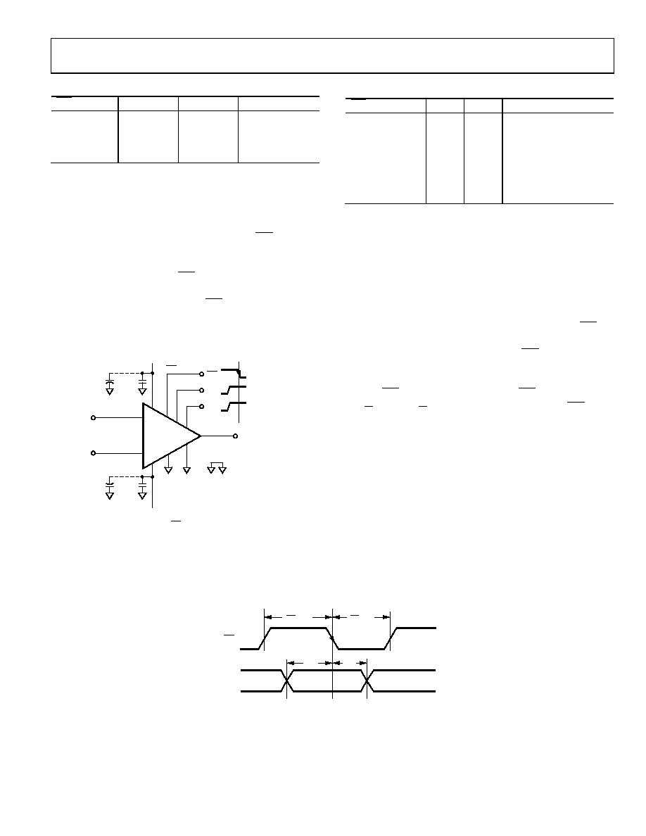
A0, A1
WR
tSU
tHD
tWR-HIGH
tWR-LOW
0
69
83
-0
53
Figure 54. Timing Diagram for Latched Gain Mode
相关PDF资料 |
PDF描述 |
|---|---|
| LT1499CS | IC OP-AMP R-R IN/OUT QUAD 14SOIC |
| TMM-105-03-LM-D | CONN HEADER 10POS DBL 2MM T/H |
| AD822BR-REEL7 | IC OPAMP GP R-R 1.9MHZ LP 8SOIC |
| MCP6406T-H/OT | IC OPAMP SGL 1.8V 1MHZ SOT23-5 |
| LTC2052HVHGN | IC OP-AMP ZERO-DRIFT QUAD 16SSOP |
相关代理商/技术参数 |
参数描述 |
|---|---|
| AD8253ARMZ-RL1 | 制造商:AD 制造商全称:Analog Devices 功能描述:10 MHz, 20 V/レs, G = 1, 10, 100, 1000 i CMOS㈢ Programmable Gain Instrumentation Amplifier |
| AD8253-EVALZ | 制造商:Analog Devices 功能描述:Evaluation Kit For 10 MHz, 20 V/US, G 1, 10, 100, 1000 CMOS Programmable Gain Instrumentation Amplifier 制造商:Analog Devices 功能描述:EVAL KIT FOR 10 MHZ, 20 V/US, G = 1, 10, 100, 1000 I CMOS PR - Boxed Product (Development Kits) |
| AD8253-EVALZ1 | 制造商:AD 制造商全称:Analog Devices 功能描述:10 MHz, 20 V/レs, G = 1, 10, 100, 1000 i CMOS㈢ Programmable Gain Instrumentation Amplifier |
| AD82550A | 制造商:AD 制造商全称:Analog Devices 功能描述:Stereo Digital Audio Amplifier with Headphone Driver |
| AD82551A | 制造商:ESMT 制造商全称:Elite Semiconductor Memory Technology Inc. 功能描述:Stereo Digital Audio Amplifier with Headphone Driver |
发布紧急采购,3分钟左右您将得到回复。