参数资料
| 型号: | AD8251ARMZ |
| 厂商: | Analog Devices Inc |
| 文件页数: | 11/24页 |
| 文件大小: | 0K |
| 描述: | IC AMP INST ICMOS LDRIFT 10MSOP |
| 标准包装: | 50 |
| 系列: | iCMOS® |
| 放大器类型: | 仪表 |
| 电路数: | 1 |
| 转换速率: | 30 V/µs |
| -3db带宽: | 10MHz |
| 电流 - 输入偏压: | 5nA |
| 电压 - 输入偏移: | 70µV |
| 电流 - 电源: | 4.1mA |
| 电流 - 输出 / 通道: | 37mA |
| 电压 - 电源,单路/双路(±): | 10 V ~ 30 V,±5 V ~ 15 V |
| 工作温度: | -40°C ~ 85°C |
| 安装类型: | 表面贴装 |
| 封装/外壳: | 10-TFSOP,10-MSOP(0.118",3.00mm 宽) |
| 供应商设备封装: | 10-MSOP |
| 包装: | 管件 |
AD8251
Rev. B | Page 19 of 24
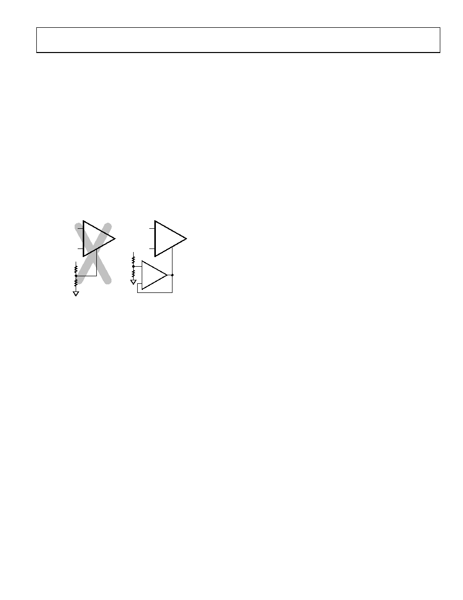
REFERENCE TERMINAL
The reference terminal, REF, is at one end of a 10 kΩ resistor
(see Figure 51). The instrumentation amplifier output is referenced
to the voltage on the REF terminal; this is useful when the output
signal needs to be offset to voltages other than its local analog
ground. For example, a voltage source can be tied to the REF
pin to level shift the output so that the AD8251 can interface
with a single-supply ADC. The allowable reference voltage
range is a function of the gain, common-mode input, and
supply voltages. The REF pin should not exceed either +VS
or VS by more than 0.5 V.
For best performance, especially in cases where the output is
not measured with respect to the REF terminal, source imped-
ance to the REF terminal should be kept low because parasitic
resistance can adversely affect CMRR and gain accuracy.
INCORRECT
AD8251
VREF
CORRECT
AD8251
OP1177
+
–
VREF
0
628
7-
0
56
Figure 57. Driving the Reference Pin
COMMON-MODE INPUT VOLTAGE RANGE
The 3-op-amp architecture of the AD8251 applies gain and then
removes the common-mode voltage. Therefore, internal nodes
in the AD8251 experience a combination of both the gained
signal and the common-mode signal. This combined signal
can be limited by the voltage supplies even when the individual
the allowable common-mode input voltage ranges for various
output voltages, supply voltages, and gains.
LAYOUT
Grounding
In mixed-signal circuits, low level analog signals need to be
isolated from the noisy digital environment. Designing with the
AD8251 is no exception. Its supply voltages are referenced to an
analog ground. Its digital circuit is referenced to a digital ground.
Although it is convenient to tie both grounds to a single ground
plane, the current traveling through the ground wires and PCB
can cause errors. Therefore, use separate analog and digital
ground planes. Analog and digital ground should meet at one
point only: star ground.
The output voltage of the AD8251 develops with respect to the
potential on the reference terminal. Take care to tie REF to the
appropriate local analog ground or to connect it to a voltage that
is referenced to the local analog ground.
Coupling Noise
To prevent coupling noise onto the AD8251, follow these
guidelines:
Do not run digital lines under the device.
Run the analog ground plane under the AD8251.
Shield fast switching signals with digital ground to avoid
radiating noise to other sections of the board, and never
run them near analog signal paths.
Avoid crossover of digital and analog signals.
Connect digital and analog ground at one point only
(typically under the ADC).
Use large traces on the power supply lines to ensure a low
impedance path. Decoupling is necessary; follow the
guidelines listed in the Power Supply Regulation and
Bypassing section.
Common-Mode Rejection
The AD8251 has high CMRR over frequency, giving it greater
immunity to disturbances, such as line noise and its associated
harmonics, in contrast to typical instrumentation amplifiers
whose CMRR falls off around 200 Hz. The typical instrumentation
amplifiers often need common-mode filters at their inputs to
compensate for this shortcoming. The AD8251 is able to reject
CMRR over a greater frequency range, reducing the need for
input common-mode filtering.
Careful board layout maximizes system performance. To
maintain high CMRR over frequency, lay out the input traces
symmetrically. Ensure that the traces maintain resistive and
capacitive balance; this holds for additional PCB metal layers
under the input pins and traces. Source resistance and capaci-
tance should be placed as close to the inputs as possible. Should
a trace cross the inputs (from another layer), it should be routed
perpendicular to the input traces.
相关PDF资料 |
PDF描述 |
|---|---|
| UY2-PK50 | SCOTCHLOK BUTT 19-26AWG 50PCS |
| TSW-149-07-L-D | CONN HEADER 98POS .100" DL GOLD |
| AD8421BRZ | IC OP AMP INSTRUMENTATION 8SOIC |
| SL1411A250SM | GAS TUBE GDT 10KA 250V SMD |
| PEC30DGBN | CONN HEADER .100 DUAL R/A 60POS |
相关代理商/技术参数 |
参数描述 |
|---|---|
| AD8251ARMZ-R7 | 功能描述:IC AMP INST ICMOS LDRIFT 10MSOP RoHS:是 类别:集成电路 (IC) >> Linear - Amplifiers - Instrumentation 系列:iCMOS® 标准包装:2,500 系列:- 放大器类型:通用 电路数:4 输出类型:- 转换速率:0.6 V/µs 增益带宽积:1MHz -3db带宽:- 电流 - 输入偏压:45nA 电压 - 输入偏移:2000µV 电流 - 电源:1.4mA 电流 - 输出 / 通道:40mA 电压 - 电源,单路/双路(±):3 V ~ 32 V,±1.5 V ~ 16 V 工作温度:0°C ~ 70°C 安装类型:表面贴装 封装/外壳:14-TSSOP(0.173",4.40mm 宽) 供应商设备封装:14-TSSOP 包装:带卷 (TR) 其它名称:LM324ADTBR2G-NDLM324ADTBR2GOSTR |
| AD8251ARMZ-RL | 功能描述:IC AMP INST ICMOS LDRIFT 10MSOP RoHS:是 类别:集成电路 (IC) >> Linear - Amplifiers - Instrumentation 系列:iCMOS® 标准包装:150 系列:- 放大器类型:音频 电路数:2 输出类型:- 转换速率:5 V/µs 增益带宽积:12MHz -3db带宽:- 电流 - 输入偏压:100nA 电压 - 输入偏移:500µV 电流 - 电源:6mA 电流 - 输出 / 通道:50mA 电压 - 电源,单路/双路(±):4 V ~ 32 V,±2 V ~ 16 V 工作温度:-40°C ~ 85°C 安装类型:表面贴装 封装/外壳:8-TSSOP(0.173",4.40mm 宽) 供应商设备封装:8-TSSOP 包装:管件 |
| AD8251ARZ | 制造商:AD 制造商全称:Analog Devices 功能描述:12MHz 20V/us G=1,2,4,8 Programmable Gain iCMOS Instrumentation Amplifier |
| AD8251ARZ-R7 | 制造商:AD 制造商全称:Analog Devices 功能描述:12MHz 20V/us G=1,2,4,8 Programmable Gain iCMOS Instrumentation Amplifier |
| AD8251ARZ-RL | 制造商:AD 制造商全称:Analog Devices 功能描述:12MHz 20V/us G=1,2,4,8 Programmable Gain iCMOS Instrumentation Amplifier |
发布紧急采购,3分钟左右您将得到回复。