参数资料
| 型号: | AD215AY |
| 厂商: | Analog Devices Inc |
| 文件页数: | 12/12页 |
| 文件大小: | 0K |
| 描述: | IC AMP ISOL LDIST 5MA 44SIP |
| 标准包装: | 1 |
| 放大器类型: | 隔离 |
| 电路数: | 1 |
| 转换速率: | 6 V/µs |
| -3db带宽: | 120kHz |
| 电流 - 输入偏压: | 300pA |
| 电压 - 输入偏移: | 400µV |
| 电流 - 电源: | 40mA |
| 电流 - 输出 / 通道: | 5mA |
| 电压 - 电源,单路/双路(±): | ±14.25 V ~ 17 V |
| 工作温度: | -40°C ~ 85°C |
| 安装类型: | 通孔 |
| 封装/外壳: | 44-SIP,12 引线,偏移引线 |
| 供应商设备封装: | 12-SIP |
| 包装: | 管件 |
AD215
REV. 0
–9–
Input Gain Adjustments for the Inverting Mode
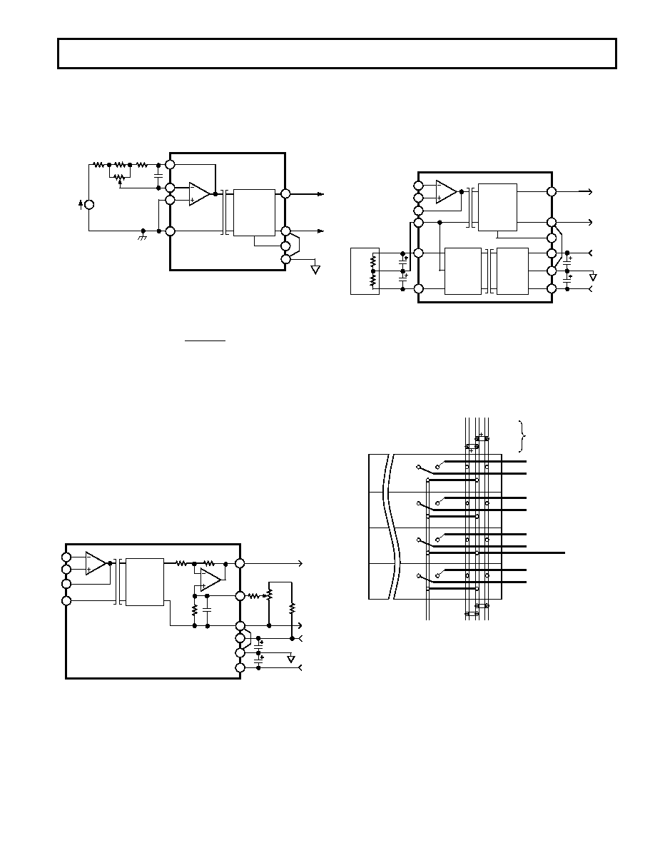
Figure 17 shows a suggested inverting gain adjustment circuit.
In this circuit, gain adjustment is made using a potentiometer
(RP) in the feedback loop. The adjustments are effective for all
gains in the 1 to 10 V/V range.
VSIGNAL
RF
RC
RIN
IN+
IN–
FB
IN COM
OUT HI
OUT LO
PWR
RTN
COM
TRIM
OUTPUT
FILTER,
BUFFER
AND
TRIM
CIRCUITRY
1
3
4
2
38
36
37
43
AD215
CF
47pF
RF
1k
Figure 17. Gain Adjustment for Inverting Configuration
For an approximate
±1% gain trim range,
RX =
RIN × RF
RIN + RF
and select
RC = 0.02
× R
IN
while
RF < 10 k
CF = 47 pF
Note: RF and RIN should have matched temperature coefficient
drift characteristics.
Output Offset Adjustments
Figure 18 illustrates one method of adjusting the output offset
voltage. Since the AD215 exhibits a nominal output offset of
–35 mV, the circuit shown was chosen to yield an offset correc-
tion of 0 mV to +73 mV. This results in a total output offset
range of approximately –35 mV to +38 mV.
IN+
IN–
FB
IN COM
OUT HI
OUT LO
COM
TRIM
LOW-PASS
FILTER,
(150k
)
1
3
4
2
38
AD215
RT
1M
RS
100k
RP2
10k
OUTPUT
BUFFER
33k
0.01F
37
36
42
+15VIN
PWR RTN
–15VIN 44
43
2.2F
–15V dc
+15V dc
Figure 18. Output Offset Adjustment Circuit
Output Gain Adjustments
Since the output amplifier stage of the AD215 is fixed at unity
gain, any adjustments can be made only in a subsequent stage.
USING ISOLATED POWER
Each AD215 provides an unregulated, isolated bipolar power
source of
±15 V dc @ ±10 mA, referred to the input common.
This source may be used to power various ancillary components
such as signal conditioning and/or adjustment circuitry, refer-
ences, op amps or remote transducers. Figure 19 shows typical
connections.
IN+
IN–
FB
IN COM
OUT HI
OUT LO
COM
TRIM
1
3
4
2
AD215
37
36
+VS
PWR
RTN
–VS
43
2.2F
–15V dc
+15V dc
+VISO
–VISO
C1
6.8F
6
C2
6.8F
5
1.5k
1.5k
LOAD
ISOLATED
DC
SUPPLY
430kHz
POWER
OSCIL-
LATOR
OUTPUT
FILTER,
BUFFER
AND
TRIM
CIRCUITRY
42
44
38
Figure 19. Using the Isolated Power Supplies
PCB LAYOUT FOR MULTICHANNEL APPLICATIONS
The pin out of the AD215 has been designed to easily facilitate
multichannel applications. Figure 20a shows a recommended
circuit board layout for a unity gain configuration.
38
36
42
44
37
43
38
36
42
44
37
43
38
36
42
44
37
43
38
36
42
44
37
43
2.2F
+15V dc
–15V dc
PWR
RTN
SUPPLY BYPASS
CAPACITORS FOR
EVERY FOUR
AD215s
OUT HI0
TRIM 0
OUT HI1
TRIM 1
OUT HI2
TRIM 2
OUT HI3
TRIM 3
ANALOG
STAR
GROUND
Figure 20a. PCB Layout for Unity Gain
CAUTION
The AD215 design does not provide short-circuit protection of
its isolated power supply. A current limiting resistor should be
placed in series with the supply terminals and the load in order
to protect against inadvertent shorts.
相关PDF资料 |
PDF描述 |
|---|---|
| AD521LDZ | IC AMP INST 40MHZ PREC LN 14CDIP |
| AD522BD | IC AMP INST 1.5KHZ LDRIFT 14CDIP |
| AD524CD | IC AMP INST 1MHZ PREC LN 16CDIP |
| AD526SD | IC AMP PGA 10MA 16CDIP |
| AD548KN | IC OPAMP GP 1MHZ LP PREC 8DIP |
相关代理商/技术参数 |
参数描述 |
|---|---|
| AD215BY | 功能描述:IC AMP ISOL LDIST 5MA 44SIP RoHS:否 类别:集成电路 (IC) >> Linear - Amplifiers - Instrumentation 系列:- 标准包装:2,500 系列:- 放大器类型:通用 电路数:4 输出类型:- 转换速率:0.6 V/µs 增益带宽积:1MHz -3db带宽:- 电流 - 输入偏压:45nA 电压 - 输入偏移:2000µV 电流 - 电源:1.4mA 电流 - 输出 / 通道:40mA 电压 - 电源,单路/双路(±):3 V ~ 32 V,±1.5 V ~ 16 V 工作温度:0°C ~ 70°C 安装类型:表面贴装 封装/外壳:14-TSSOP(0.173",4.40mm 宽) 供应商设备封装:14-TSSOP 包装:带卷 (TR) 其它名称:LM324ADTBR2G-NDLM324ADTBR2GOSTR |
| AD215BY | 制造商:Analog Devices 功能描述:IC AMP ISOLATION |
| AD215BYZ | 制造商:Analog Devices 功能描述:ISOLATION AMPLIFIER IC PACKAGE/CASE:12-S |
| AD-2164S | 制造商:BOTHHAND 制造商全称:Bothhand USA, LP. 功能描述:ADSL LINE TRANSFORMER |
| AD2-165Q-30000281 | 制造商:Amphenol Commercial 功能描述:RACK & PANEL CONNECTOR 制造商:Amphenol Corporation 功能描述:RACK AND PANEL CONNECTOR |
发布紧急采购,3分钟左右您将得到回复。