参数资料
| 型号: | AD204KY |
| 厂商: | Analog Devices Inc |
| 文件页数: | 7/12页 |
| 文件大小: | 0K |
| 描述: | IC AMP ISOL 5KHZ QUAD LP 38SIP |
| 标准包装: | 1 |
| 放大器类型: | 隔离 |
| 电路数: | 4 |
| 增益带宽积: | 5kHz |
| 电流 - 输入偏压: | 30pA |
| 电压 - 输入偏移: | 5000µV |
| 电流 - 输出 / 通道: | 2mA |
| 工作温度: | 0°C ~ 70°C |
| 安装类型: | 通孔 |
| 封装/外壳: | 38-SIP,10 引线,偏移引线 |
| 供应商设备封装: | 10-SIP |
| 包装: | 管件 |
REV. D
AD202/AD204
–4–
DIFFERENCES BETWEEN THE AD202 AND AD204
The primary distinction between the AD202 and AD204 is in
the method by which they are powered: the AD202 operates
directly from 15 V dc while the AD204 is powered by a non-
isolated externally-supplied clock (AD246) that can drive up to
32 AD204s. The main advantages of using the externally-
clocked AD204 over the AD202 are reduced cost in multichannel
applications, lower power consumption, and higher bandwidth.
In addition, the AD204 can supply substantially more isolated
power than the AD202.
Of course, in a great many situations, especially where only one
or a few isolators are used, the convenience of standalone opera-
tion provided by the AD202 will be more significant than any
of the AD204’s advantages. There may also be cases where it is
desirable to accommodate either device interchangeably, so the
pinouts of the two products have been designed to make that
easy to do.
RECT
AND
FILTER
OSCILLATOR
DEMOD
MOD
SIGNAL
POWER
5V
FS
+7.5V
–7.5V
25kHz
AD202
FB
IN–
IN+
IN COM
VSIG
+VISO OUT
–VISO OUT
5V
FS
HI
LO
15V DC
POWER
RETURN
VOUT
Figure 1a. AD202 Functional Block Diagram
RECT
AND
FILTER
POWER
CONV.
DEMOD
MOD
SIGNAL
POWER
5V
FS
+7.5V
–7.5V
25kHz
AD204
FB
IN–
IN+
IN COM
VSIG
+VISO OUT
–VISO OUT
5V
FS
HI
LO
CLOCK
15V p-p
25kHz
POWER
RETURN
VOUT
Figure 1b. AD204 Functional Block Diagram
(Pin Designations Apply to the DIP-Style Package)
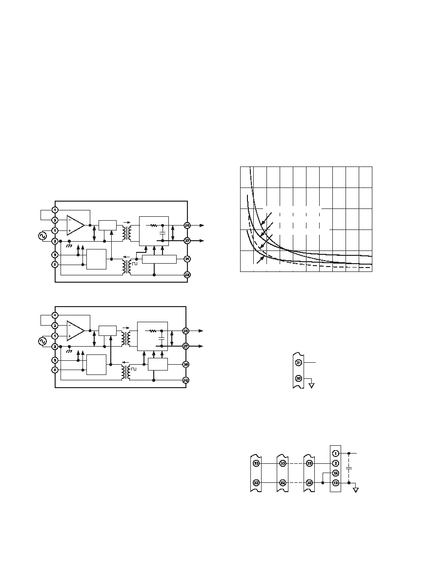
INSIDE THE AD202 AND AD204
The AD202 and AD204 use an amplitude modulation technique
to permit transformer coupling of signals down to dc (Figure 1a
and 1b). Both models also contain an uncommitted input op
amp and a power transformer that provides isolated power to
the op amp, the modulator, and any external load. The power
transformer primary is driven by a 25 kHz, 15 V p-p square
wave generated internally in the case of the AD202, or supplied
externally for the AD204.
Within the signal swing limits of approximately
±5 V, the out-
put voltage of the isolator is equal to the output voltage of the
op amp; that is, the isolation barrier has unity gain. The output
signal is not internally buffered, so the user is free to interchange
the output leads to get signal inversion. Additionally, in multi-
channel applications, the unbuffered outputs can be multiplexed
with one buffer following the mux. This technique minimizes
offset errors while reducing power consumption and cost. The
output resistance of the isolator is typically 3 k
for the AD204
(7 k
for AD202) and varies with signal level and temperature,
so it should not be loaded (see Figure 2 for the effects of load
upon nonlinearity and gain drift). In many cases, a high imped-
ance load will be present or a following circuit such as an output
filter can serve as a buffer so that a separate buffer function will
not often be needed.
OUTPUT LOAD – M
0.25
0.20
0
1.0
0.1
0.2
0.3
0.4
0.5
0.6
0.7
0.8
0.9
0.15
0.10
0.05
–10
–8
–6
–4
–2
0
–500
–400
–300
–200
–100
0
GAIN
CHANGE
(%)
GAIN TC
CHANGE
(ppm/ C)
NON-
LINEARITY
(%)
AD202 GAIN AND GAIN TC
AD202 NONLINEARITY
AD204 NONLINEARITY
AD204 GAIN AND GAIN TC
Figure 2. Effects of Output Loading
USING THE AD202 AND AD204
Powering the AD202. The AD202 requires only a single 15 V
power supply connected as shown in Figure 3a. A bypass capaci-
tor is provided in the module.
15V
5%
15V RETURN
AD202
Figure 3a.
Powering the AD204. The AD204 gets its power from an
externally supplied clock signal (a 15 V p-p square wave with a
nominal frequency of 25 kHz) as shown in Figure 3b.
15V
15V RETURN
AD204
AD246
+
Figure 3b.
(NOTE: Circuit figures shown on this page are for SIP-style packages. Refer to
Page 3 for proper DIP package pinout.)
相关PDF资料 |
PDF描述 |
|---|---|
| AD208BY | IC AMP ISOL 4KHZ PREC 2MA 38SIP |
| AD210JN | IC AMP ISOL PREC LDRIFT 38DIP |
| AD215AY | IC AMP ISOL LDIST 5MA 44SIP |
| AD521LDZ | IC AMP INST 40MHZ PREC LN 14CDIP |
| AD522BD | IC AMP INST 1.5KHZ LDRIFT 14CDIP |
相关代理商/技术参数 |
参数描述 |
|---|---|
| AD205-00E | 功能描述:SENSOR MAG SW 40G STANDRD 8-MSOP 制造商:nve corp/sensor products 系列:AD 包装:管件 零件状态:有效 功能:全极开关 技术:霍尔效应 极化:任意一种 感应范围:±2.5mT 跳闸,±1.1mT 释放 测试条件:-40°C ~ 125°C 电压 - 电源:4.5 V ~ 30 V 电流 - 电源(最大值):4.5mA 电流 - 输出(最大值):20mA 输出类型:开路集电极 特性:- 工作温度:-40°C ~ 125°C(TA) 封装/外壳:8-TSSOP,8-MSOP(0.118",3.00mm 宽) 供应商器件封装:8-MSOP 标准包装:1,000 |
| AD205-02E | 功能描述:SENSOR MAG SW 40G STANDARD 8SOIC 制造商:nve corp/sensor products 系列:AD 包装:管件 零件状态:有效 功能:全极开关 技术:霍尔效应 极化:任意一种 感应范围:±5mT 跳闸,±2.5mT 释放 测试条件:-40°C ~ 125°C 电压 - 电源:4.5 V ~ 30 V 电流 - 电源(最大值):4.5mA 电流 - 输出(最大值):20mA 输出类型:开路集电极 特性:- 工作温度:-40°C ~ 125°C(TA) 封装/外壳:8-SOIC(0.154",3.90mm 宽) 供应商器件封装:8-SOIC 标准包装:1,000 |
| AD2051/1 | 制造商:Analog Devices 功能描述: |
| AD205MX-G50GLF | 制造商:ADDA USA Corporation 功能描述:AD Series 20 x 20 x 6 mm 5 V 2.3 CFM Hypro Bearing DC Fan |
| AD206-00E | 功能描述:SENSOR MAG SW 80G STANDRD 8-MSOP 制造商:nve corp/sensor products 系列:AD 包装:管件 零件状态:有效 功能:全极开关 技术:霍尔效应 极化:任意一种 感应范围:±10mT 跳闸,±6.5mT 释放 测试条件:-40°C ~ 125°C 电压 - 电源:4.5 V ~ 30 V 电流 - 电源(最大值):4.5mA 电流 - 输出(最大值):20mA 输出类型:开路集电极 特性:- 工作温度:-40°C ~ 125°C(TA) 封装/外壳:8-TSSOP,8-MSOP(0.118",3.00mm 宽) 供应商器件封装:8-MSOP 标准包装:1,000 |
发布紧急采购,3分钟左右您将得到回复。