- 您现在的位置:买卖IC网 > PDF目录42519 > 97042-11 (PEREGRINE SEMICONDUCTOR CORP) PHASE LOCKED LOOP, 300 MHz, CQCC44 PDF资料下载
参数资料
| 型号: | 97042-11 |
| 厂商: | PEREGRINE SEMICONDUCTOR CORP |
| 元件分类: | PLL合成/DDS/VCOs |
| 英文描述: | PHASE LOCKED LOOP, 300 MHz, CQCC44 |
| 封装: | CERAMIC, QFJ-44 |
| 文件页数: | 4/11页 |
| 文件大小: | 456K |
| 代理商: | 97042-11 |
Product Specification
PE97042
Page 2 of 11
2007-2011 Peregrine Semiconductor Corp. All rights reserved.
Document No. 70-0236-05
│ UltraCMOS RFIC Solutions
C
LOC
K,
M
6
GND
R
3
R
2
R
1
R
0
V
DD
LD
EN
H
F
R
GND
M
7
M
8
A
0
D
MO
DE
V
DD
E_W
R
,A
1
A
2
A
3
F
IN
F
IN
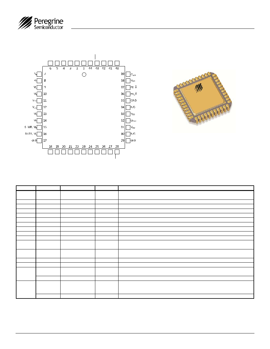
Table 1. Pin Descriptions
Figure 2. Pin Configurations (Top View)
44-lead CQFJ
Figure 3. Package Type
Pin No.
Pin Name
Interface Mode
Type
Description
1
VDD
Both
(Note 1)
Power supply input. Input may range from 2.85 V to 3.45 V. Bypassing
recommended.
2
R0
Direct
Input
R Counter bit0
3
R1
Direct
Input
R Counter bit1
4
R2
Direct
Input
R Counter bit2
5
R3
Direct
Input
R Counter bit3
6
GND
Both
Ground
7
R4
Direct
Input
R Counter bit4
8
R5
Direct
Input
R Counter bit5 (MSB)
9
M0
Direct
Input
M Counter bit0
10
M1
Direct
Input
M Counter bit1
11
VDD
Both
(Note 1)
Power supply input. Input may range from 2.85 V to 3.45 V. Bypassing
recommended.
12
VDD
Both
(Note 1)
Power supply input. Input may range from 2.85 V to 3.45 V. Bypassing
recommended.
13
M2
Direct
Input
M Counter bit2
14
M3
Direct
Input
M Counter bit3
15
S_WR
Serial
Input
Frequency register load enable input. Buffered data is transferred to the frequency
register on S_WR rising edge.
M4
Direct
Input
M Counter bit4
16
DATA
Serial
Input
Binary serial data input. Data is entered LSB first, and is clocked serially into the 20
-bit frequency control register (E_WR “low”) or the 8-bit enhancement register
(E_WR “high”) on the rising edge of CLOCK.
M5
Direct
Input
M Counter bit5
相关PDF资料 |
PDF描述 |
|---|---|
| 97042-99 | PHASE LOCKED LOOP, 300 MHz, UUC |
| 97050-1020 | PZA320, IC SOCKET |
| 97050-2121 | PZA320, IC SOCKET |
| 97050-1021 | PZA320, IC SOCKET |
| 97050-2120 | PZA320, IC SOCKET |
相关代理商/技术参数 |
参数描述 |
|---|---|
| 97042119 | 制造商:Laird Technologies Inc 功能描述:CSTR FRG NIB |
| 97042304 | 制造商:Laird Technologies Inc 功能描述:CSTR FRG AG |
| 97042402 | 制造商:Laird Technologies Inc 功能描述:CSTR FRG BF |
| 97043-00000 | 功能描述:PELTOR SPORT SOUNDTRAP/TACTICAL 制造商:3m 系列:* 零件状态:在售 标准包装:1 |
| 97043002 | 制造商:Laird Technologies Inc 功能描述:CSTR STR BF |
发布紧急采购,3分钟左右您将得到回复。