- 您现在的位置:买卖IC网 > PDF目录25515 > 952906AGLFT (INTEGRATED DEVICE TECHNOLOGY INC) 400 MHz, PROC SPECIFIC CLOCK GENERATOR, PDSO48 PDF资料下载
参数资料
| 型号: | 952906AGLFT |
| 厂商: | INTEGRATED DEVICE TECHNOLOGY INC |
| 元件分类: | 时钟产生/分配 |
| 英文描述: | 400 MHz, PROC SPECIFIC CLOCK GENERATOR, PDSO48 |
| 封装: | 6.10 MM, 0.50 MM PITCH, ROHS COMPLIANT, MO-153, TSSOP-48 |
| 文件页数: | 13/23页 |
| 文件大小: | 301K |
| 代理商: | 952906AGLFT |
20
Integrated
Circuit
Systems, Inc.
ICS952906A
1236A—08/06/07
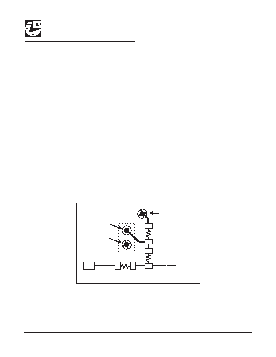
Fig. 1
Shared Pin Operation -
Input/Output Pins
The I/O pins designated by (input/output) serve as dual
signal functions to the device. During initial power-up, they
act as input pins. The logic level (voltage) that is present on
these pins at this time is read and stored into a 5-bit internal
data latch. At the end of Power-On reset, (see AC
characteristics for timing values), the device changes the
mode of operations for these pins to an output function. In
this mode the pins produce the specified buffered clocks to
external loads.
To program (load) the internal configuration register for
these pins, a resistor is connected to either the VDD (logic 1)
power supply or the GND (logic 0) voltage potential. A 10
Kilohm (10K) resistor is used to provide both the solid CMOS
programming voltage needed during the power-up
programming period and to provide an insignificant load on
the output clock during the subsequent operating period.
Via to
VDD
Clock trace to load
Series Term. Res.
Programming
Header
Via to Gnd
Device
Pad
2K
W
8.2K
W
Figure 1 shows a means of implementing this function
when a switch or 2 pin header is used. With no jumper is
installed the pin will be pulled high. With the jumper in
place the pin will be pulled low. If programmability is not
necessary, than only a single resistor is necessary. The
programming resistors should be located close to the series
termination resistor to minimize the current loop area. It is
more important to locate the series termination resistor
close to the driver than the programming resistor.
相关PDF资料 |
PDF描述 |
|---|---|
| 952906AFLFT | 400 MHz, PROC SPECIFIC CLOCK GENERATOR, PDSO48 |
| 953002DFLF | 400 MHz, PROC SPECIFIC CLOCK GENERATOR, PDSO56 |
| 953002CFLFT | 400 MHz, PROC SPECIFIC CLOCK GENERATOR, PDSO56 |
| 953220640112 | TELECOM, CORDLESS, BASEBAND CIRCUIT, PDSO16 |
| 953220640118 | TELECOM, CORDLESS, BASEBAND CIRCUIT, PDSO16 |
相关代理商/技术参数 |
参数描述 |
|---|---|
| 952906BFLF | 功能描述:时钟发生器及支持产品 RoHS:否 制造商:Silicon Labs 类型:Clock Generators 最大输入频率:14.318 MHz 最大输出频率:166 MHz 输出端数量:16 占空比 - 最大:55 % 工作电源电压:3.3 V 工作电源电流:1 mA 最大工作温度:+ 85 C 安装风格:SMD/SMT 封装 / 箱体:QFN-56 |
| 952906BFLFT | 功能描述:时钟发生器及支持产品 RoHS:否 制造商:Silicon Labs 类型:Clock Generators 最大输入频率:14.318 MHz 最大输出频率:166 MHz 输出端数量:16 占空比 - 最大:55 % 工作电源电压:3.3 V 工作电源电流:1 mA 最大工作温度:+ 85 C 安装风格:SMD/SMT 封装 / 箱体:QFN-56 |
| 952906BGLF | 功能描述:时钟发生器及支持产品 RoHS:否 制造商:Silicon Labs 类型:Clock Generators 最大输入频率:14.318 MHz 最大输出频率:166 MHz 输出端数量:16 占空比 - 最大:55 % 工作电源电压:3.3 V 工作电源电流:1 mA 最大工作温度:+ 85 C 安装风格:SMD/SMT 封装 / 箱体:QFN-56 |
| 952906BGLFT | 功能描述:时钟发生器及支持产品 RoHS:否 制造商:Silicon Labs 类型:Clock Generators 最大输入频率:14.318 MHz 最大输出频率:166 MHz 输出端数量:16 占空比 - 最大:55 % 工作电源电压:3.3 V 工作电源电流:1 mA 最大工作温度:+ 85 C 安装风格:SMD/SMT 封装 / 箱体:QFN-56 |
| 952909AKLF | 制造商:Integrated Device Technology Inc 功能描述:PROGRAMMABLE-TIMING-CONTROL-HUB-NEXT-GEN-P4-PROCESSOR 制造商:Integrated Device Technology Inc 功能描述:PC MAIN CLOCK, MLF56 - Trays |
发布紧急采购,3分钟左右您将得到回复。