- 您现在的位置:买卖IC网 > PDF目录25515 > 952906AFT (INTEGRATED DEVICE TECHNOLOGY INC) 400 MHz, PROC SPECIFIC CLOCK GENERATOR, PDSO48 PDF资料下载
参数资料
| 型号: | 952906AFT |
| 厂商: | INTEGRATED DEVICE TECHNOLOGY INC |
| 元件分类: | 时钟产生/分配 |
| 英文描述: | 400 MHz, PROC SPECIFIC CLOCK GENERATOR, PDSO48 |
| 封装: | MO-118, SSOP-48 |
| 文件页数: | 23/23页 |
| 文件大小: | 301K |
| 代理商: | 952906AFT |
9
Integrated
Circuit
Systems, Inc.
ICS952906A
1236A—08/06/07
I
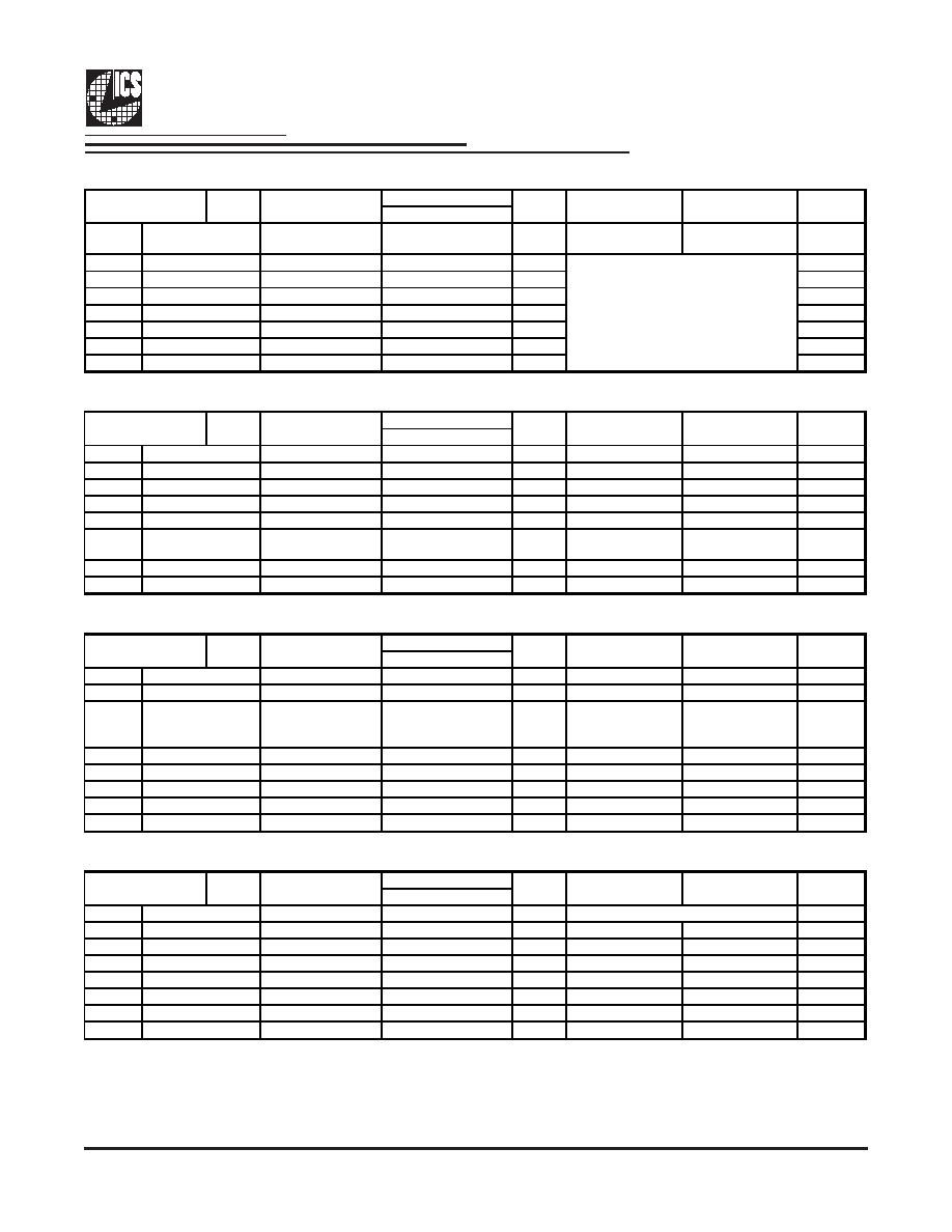
2C Table: Frequency Select Register
Control
Function
Bit 7
FS Source
Frequency H/W IIC
Select
RW
0
Bit 6
FS6
Freq Select Bit 6
RW
0
Bit 5
FS5
Freq Select Bit 5
RW
0
Bit 4
FS4
Freq Select Bit 4
RW
0
Bit 3
FS3
Freq Select Bit 3
RW
0
Bit 2
FS2
Freq Select Bit 2
RW
0
Bit 1
FS1
Freq Select Bit 1
RW
0
Bit 0
FS0
Freq Select Bit 0
RW
0
I
2C Table: Spreading and Device Behavior Control Register
Control
Function
Bit 7
SS1
Spread Select 1**
RW
0
Bit 6
SS0
Spread Select 0**
RW
1
Bit 5
SS_EN
Spread Enable Control
RW
1
Bit 4
WDS_EN
WD Soft Reset Enable
RW
0
Bit 3
Reserved
RW
1
Bit 2
CPUCLKT/C_ITP,
CPU1T/C, CPU0T/C
Output Control
RW
1
Bit 1
CPUCLKT/C_1
Output Control
RW
1
Bit 0
CPUCLKT/C_0
Output Control
RW
1
I
2C Table: Output Control Register
Control
Function
Bit 7
25MHz_0
Output Control
RW
1
Bit 6
25MHz_1
Output Control
RW
1
Bit 5
CPUT Stop Mode
0: CPUT Driven during
PD#; 1: Tri-stated
RW
0
Bit 4
Reserved
RW
1
Bit 3
3V66_1
Output Control
RW
1
Bit 2
Reserved
RW
1
Bit 1
CPUCLKT/C_1
Output Stop Control
RW
1
Bit 0
CPUCLKT/C_0
Output Stop Control
RW
1
I
2C Table: Output Control Register
Control
Function
Bit 7
ASEL1
3V66/PCI Freq Select
RW
0
Bit 6
PCICLK6
Output Control
RW
1
Bit 5
PCICLK5
Output Control
RW
1
Bit 4
PCICLK4
Output Control
RW
1
Bit 3
PCICLK3
Output Control
RW
1
Bit 2
PCICLK2
Output Control
RW
1
Bit 1
PCICLK1
Output Control
RW
1
Bit 0
PCICLK0
Output Control
RW
1
Disable
Enable
See Table 5: Async AGP/PCI Freq Table
Disable
Enable
Disable
Enable
Disable
Enable
Disable
Enable
Disable
Enable
Free Run
Stoppable
Disable
Enable
--
Free Run
Stoppable
Disable
Enable
Disable
Enable
--
Disable
Enable
Driven
Hi-Z
Disable
Enable
Disable
Enable
ON
OFF
--
01 = 0.25%
Reserved
PWD
-
Byte 3
Pin #
Name
Type
0
1
36
35
26
-
42,41
39, 38
20
Type
PWD
39, 38
Byte 2
Pin #
Name
0
1
** Spread program m ing only applies for ROM table entries 0001000 to 0001011 and 0010000 to 0010111
-
45, 44
42,41
ON
OFF
-
PWD
-
Byte 1
Pin #
Name
Type
00 = 0.20%
10 = 0.35%
-
See Table 1: QuadRom Frequency
Selection Table
01
PWD
-
Byte 0
Pin #
Name
Type
Latch Inputs
IIC
01
-
19
16
15
14
13
12
-
相关PDF资料 |
PDF描述 |
|---|---|
| 952906AGLFT | 400 MHz, PROC SPECIFIC CLOCK GENERATOR, PDSO48 |
| 952906AFLFT | 400 MHz, PROC SPECIFIC CLOCK GENERATOR, PDSO48 |
| 953002DFLF | 400 MHz, PROC SPECIFIC CLOCK GENERATOR, PDSO56 |
| 953002CFLFT | 400 MHz, PROC SPECIFIC CLOCK GENERATOR, PDSO56 |
| 953220640112 | TELECOM, CORDLESS, BASEBAND CIRCUIT, PDSO16 |
相关代理商/技术参数 |
参数描述 |
|---|---|
| 952906AGLF | 功能描述:时钟发生器及支持产品 RoHS:否 制造商:Silicon Labs 类型:Clock Generators 最大输入频率:14.318 MHz 最大输出频率:166 MHz 输出端数量:16 占空比 - 最大:55 % 工作电源电压:3.3 V 工作电源电流:1 mA 最大工作温度:+ 85 C 安装风格:SMD/SMT 封装 / 箱体:QFN-56 |
| 952906AGLFT | 功能描述:时钟发生器及支持产品 RoHS:否 制造商:Silicon Labs 类型:Clock Generators 最大输入频率:14.318 MHz 最大输出频率:166 MHz 输出端数量:16 占空比 - 最大:55 % 工作电源电压:3.3 V 工作电源电流:1 mA 最大工作温度:+ 85 C 安装风格:SMD/SMT 封装 / 箱体:QFN-56 |
| 952906BFLF | 功能描述:时钟发生器及支持产品 RoHS:否 制造商:Silicon Labs 类型:Clock Generators 最大输入频率:14.318 MHz 最大输出频率:166 MHz 输出端数量:16 占空比 - 最大:55 % 工作电源电压:3.3 V 工作电源电流:1 mA 最大工作温度:+ 85 C 安装风格:SMD/SMT 封装 / 箱体:QFN-56 |
| 952906BFLFT | 功能描述:时钟发生器及支持产品 RoHS:否 制造商:Silicon Labs 类型:Clock Generators 最大输入频率:14.318 MHz 最大输出频率:166 MHz 输出端数量:16 占空比 - 最大:55 % 工作电源电压:3.3 V 工作电源电流:1 mA 最大工作温度:+ 85 C 安装风格:SMD/SMT 封装 / 箱体:QFN-56 |
| 952906BGLF | 功能描述:时钟发生器及支持产品 RoHS:否 制造商:Silicon Labs 类型:Clock Generators 最大输入频率:14.318 MHz 最大输出频率:166 MHz 输出端数量:16 占空比 - 最大:55 % 工作电源电压:3.3 V 工作电源电流:1 mA 最大工作温度:+ 85 C 安装风格:SMD/SMT 封装 / 箱体:QFN-56 |
发布紧急采购,3分钟左右您将得到回复。