- 您现在的位置:买卖IC网 > PDF目录25515 > 952801CFLFT (INTEGRATED DEVICE TECHNOLOGY INC) 293.34 MHz, PROC SPECIFIC CLOCK GENERATOR, PDSO48 PDF资料下载
参数资料
| 型号: | 952801CFLFT |
| 厂商: | INTEGRATED DEVICE TECHNOLOGY INC |
| 元件分类: | 时钟产生/分配 |
| 英文描述: | 293.34 MHz, PROC SPECIFIC CLOCK GENERATOR, PDSO48 |
| 封装: | MO-118, GREEN, SSOP-48 |
| 文件页数: | 3/24页 |
| 文件大小: | 219K |
| 代理商: | 952801CFLFT |
11
Integrated
Circuit
Systems, Inc.
ICS952801
Advance Information
0719—01/22/03
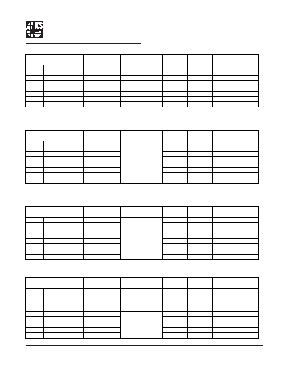
I
2C Table: Output Control Register
Control
Function
Bit 7
PCICLK_F1
Output Control
RW
Disable
Enable
1
Bit 6
PCICLK_F0
Output Control
RW
Disable
Enable
1
Bit 5
PCICLK5
Output Control
RW
Disable
Enable
1
Bit 4
PCICLK4
Output Control
RW
Disable
Enable
1
Bit 3
PCICLK3
Output Control
RW
Disable
Enable
1
Bit 2
PCICLK2
Output Control
RW
Disable
Enable
1
Bit 1
PCICLK1
Output Control
RW
Disable
Enable
1
Bit 0
PCICLK0
Output Control
RW
Disable
Enable
1
I
2C Table: Byte Count Register
Control
Function
Bit 7
BC7
RW
-
0
Bit 6
BC6
RW
-
0
Bit 5
BC5
RW
-
0
Bit 4
BC4
RW
-
0
Bit 3
BC3
RW
-
1
Bit 2
BC2
RW
-
1
Bit 1
BC1
RW
-
1
Bit 0
BC0
RW
-
1
I
2C Table: Watchdog Timer Register
Control
Function
Bit 7
WD7
RW
-
0
Bit 6
WD6
RW
-
0
Bit 5
WD5
RW
-
0
Bit 4
WD4
RW
-
1
Bit 3
WD3
RW
-
0
Bit 2
WD2
RW
-
0
Bit 1
WD1
RW
-
0
Bit 0
WD0
RW
-
0
I
2C Table: VCO Control Select Bit & WD Timer Control Register
Control
Function
Bit 6
WDEN
Watchdog Enable
R
Disable
Enable
0
Bit 5
Reserved
RW
-
0
Bit 4
WD SF4
RW
-
0
Bit 3
WD SF3
RW
-
0
Bit 2
WD SF2
RW
-
0
Bit 1
WD SF1
RW
-
0
Bit 0
WD SF0
RW
-
1
Type
Byte 9
Pin #
Name
1
0
Disable
0
PWD
1
01
0
Enable
PWD
14
Type
Name
0
1
13
22
21
Byte 7
Pin #
Byte 8
Pin #
Name
20
19
18
17
PWD
-
Writing to this register
will configure how
many bytes will be read
back, default is 0F = 15
bytes.
-
These bits represent
X*290ms the watchdog
timer will wait before it
goes to alarm mode.
Default is 16 X 290ms
=4.64 seconds
-
Byte 10
Pin #
Bit 7
-M/NEN
M/N Programming
Enable
Name
Type
RW
-
Writing to these bit will
configure the safe
frequency as Byte4bit
2, (7:4), Byte 24bit(6:5)
-
相关PDF资料 |
PDF描述 |
|---|---|
| 952807 | MODULAR TERMINAL BLOCK |
| 9528090000 | 10 A, MODULAR TERMINAL BLOCK, 1 DECK |
| 952830 | MODULAR TERMINAL BLOCK |
| 49830 | MODULAR TERMINAL BLOCK |
| 49810 | MODULAR TERMINAL BLOCK |
相关代理商/技术参数 |
参数描述 |
|---|---|
| 95280-302LF | 制造商:FCI 功能描述: |
| 95280-303LF | 制造商:FCI 功能描述: |
| 95280-304LF | 制造商:FCI 功能描述: |
| 9-528040-0 | 功能描述:DIE SET FOR HVC 70/2 X 6MM2 制造商:te connectivity amp connectors 系列:* 零件状态:有效 标准包装:1 |
| 9-528040-4 | 功能描述:DIE SET HV 90 AK SHIELD CRIMP 35 制造商:te connectivity amp connectors 系列:* 零件状态:有效 标准包装:1 |
发布紧急采购,3分钟左右您将得到回复。