- 您现在的位置:买卖IC网 > PDF目录24864 > 950902DGLFT (INTEGRATED DEVICE TECHNOLOGY INC) 200.4 MHz, PROC SPECIFIC CLOCK GENERATOR, PDSO56 PDF资料下载
参数资料
| 型号: | 950902DGLFT |
| 厂商: | INTEGRATED DEVICE TECHNOLOGY INC |
| 元件分类: | 时钟产生/分配 |
| 英文描述: | 200.4 MHz, PROC SPECIFIC CLOCK GENERATOR, PDSO56 |
| 封装: | 6.10 MM, 0.50 MM PITCH, MO-153, TSSOP-56 |
| 文件页数: | 5/22页 |
| 文件大小: | 210K |
| 代理商: | 950902DGLFT |
13
Integrated
Circuit
Systems, Inc.
ICS950902
0475F—10/13/03
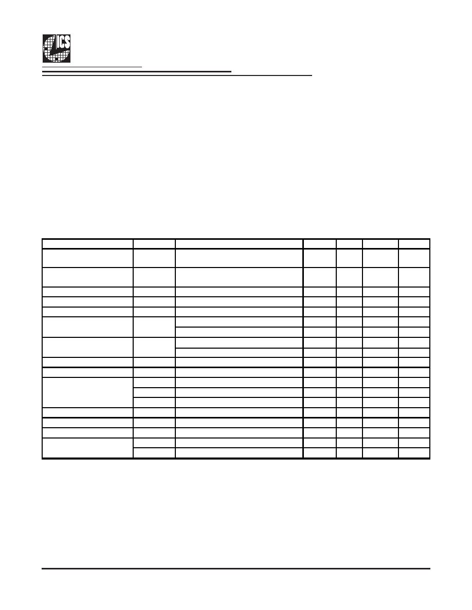
Absolute Maximum Ratings
Supply Voltage . . . . . . . . . . . . . . . . . . . . . . . . . . . 5.5 V
Logic Inputs . . . . . . . . . . . . . . . . . . . . . . . . . . . . . GND –0.5 V to VDD +0.5 V
Ambient Operating Temperature . . . . . . . . . . . . 0°C to +70°C
Case Temperature . . . . . . . . . . . . . . . . . . . . . . . . 115°C
Storage Temperature . . . . . . . . . . . . . . . . . . . . . –65°C to +150°C
Stresses above those listed under
Absolute Maximum Ratings may cause permanent damage to the device. These ratings are
stress specifications only and functional operation of the device at these or any other conditions above those listed in the
operational sections of the specifications is not implied. Exposure to absolute maximum rating conditions for extended
periods may affect product reliability.
Electrical Characteristics- Input/Supply/Common Output Parameters
TA = 0 - 70°C; Supply Voltage VDD = 3.3V +-5%
PARAMETER
SYMBOL
CONDITIONS
MIN
TYP
MAX
UNITS
Input High Voltage
VIH
2
VDD + 0.3
V
Input Low Voltage
VIL
VSS - 0.3
0.8
V
Input High Current
IIH
VIN =VDD
-5
5
mA
Input Low Current
IIL1
VIN= 0 V; Inputs with no pull-up
-5
mA
Input Low Current
IIL2
VIN= 0 V; Inputs with no pull-up
-200
mA
CL= 0 pF; Select @ 66M
100
mA
CL = Full load @ 133Mhz
156
280
mA
IREF=2.32
10
20
mA
IREF= 5mA
37
mA
Input frequency
Fi
VDD=3.3V;
MHz
Pin Inductance
Lpin
7nH
CIN
Logic Inputs
5
pF
Cout
Output pin capacitance
6
pF
CINX
X1 & X2 pins
27
45
pF
Transition Time1
Ttrans
To 1st crossing of target Freq.
3
ms
Settling Time1
Ts
From 1st crossing to 1% target Freq.
3
ms
Clk Stabilization1
TSTAB
From VDD = 3.3 V to 1% target Freq.
3ms
tPZH,tPZH
output enable delay (all outputs)
1
10
ns
tPLZ,tPZH
output disable delay (all outputs)
1
10
ns
1Guaranteed by design, not 100% tested in production.
Capacitance1
Delay
IDD3.3OP
Operating Supply Current
Power Down Supply
Current
IDD3.3PD
相关PDF资料 |
PDF描述 |
|---|---|
| 08056C103JAT7A | Separating plate, width: 0.8 mm, color: gray - TS-GSK |
| 08056C103JAT9A | General Specifications |
| 950902DGLF | 200.4 MHz, PROC SPECIFIC CLOCK GENERATOR, PDSO56 |
| 08056C103KA72A | General Specifications |
| 950908BGLF | 200.4 MHz, PROC SPECIFIC CLOCK GENERATOR, PDSO56 |
相关代理商/技术参数 |
参数描述 |
|---|---|
| 9509060100 | 制造商:未知厂家 制造商全称:未知厂家 功能描述:Computer Cable for EIA RS-232 Applications |
| 95090601000 | 制造商:未知厂家 制造商全称:未知厂家 功能描述:Computer Cable for EIA RS-232 Applications |
| 9509060500 | 制造商:未知厂家 制造商全称:未知厂家 功能描述:Computer Cable for EIA RS-232 Applications |
| 950-908 | 制造商:Mitutoyo Corporation 功能描述:TOOL KIT, MACHINIST |
| 950908BF | 制造商:Ics 功能描述:200.4 MHz, PROC SPECIFIC CLOCK GENERATOR, 56 Pin Plastic SMT |
发布紧急采购,3分钟左右您将得到回复。