- 您现在的位置:买卖IC网 > PDF目录24844 > 93V850DGT (INTEGRATED DEVICE TECHNOLOGY INC) 93V SERIES, PLL BASED CLOCK DRIVER, 10 TRUE OUTPUT(S), 0 INVERTED OUTPUT(S), PDSO48 PDF资料下载
参数资料
| 型号: | 93V850DGT |
| 厂商: | INTEGRATED DEVICE TECHNOLOGY INC |
| 元件分类: | 时钟及定时 |
| 英文描述: | 93V SERIES, PLL BASED CLOCK DRIVER, 10 TRUE OUTPUT(S), 0 INVERTED OUTPUT(S), PDSO48 |
| 封装: | 0.240 INCH, MO-153, TSSOP-48 |
| 文件页数: | 5/10页 |
| 文件大小: | 194K |
| 代理商: | 93V850DGT |
4
ICS93V850
Preliminary Product Preview
0423H—07/03/03
Absolute Maximum Ratings
Supply Voltage: (VDD & AVDD) . . . . . . . . . . . . . . . -0.5V to 3.6V
(VDDI) . . . . . . . . . . . . . . . . . . . -0.5V to 4.6V
Logic Inputs: VI (except SCLK and SDATA) . . . . . . –0.5 V to VDD +0.5 V
VI (SCLK and SDATA) . . . . . . . . . –0.5 V to VDDI2C +0.5 V
Logic Outputs: VO (except SDATA) . . . . . . . . . . . . . –0.5 V to VDD +0.5 V
VO (SDATA) . . . . . . . . . . . . . . . . –0.5 V to VDDI2C +0.5 V
Input clamp current: IIK (VI < 0 or VI > VDD) . . . . +/- 50mA
Output clamp current: IOK (VO < 0 or VO > VDD) +/- 50mA
Continuous output current: IO (VO = 0 to VDD) . . +/- 50mA
Package thermal impedance, theta JA: DGG package +89°C/W
Storage Temperature . . . . . . . . . . . . . . . . . . . . . . . . –65°C to +150°C
Stresses above those listed under
Absolute Maximum Ratings may cause permanent damage to the device. These
ratings are stress specifications only and functional operation of the device at these or any other conditions above
those listed in the operational sections of the specifications is not implied. Exposure to absolute maximum rating
conditions for extended periods may affect product reliability.
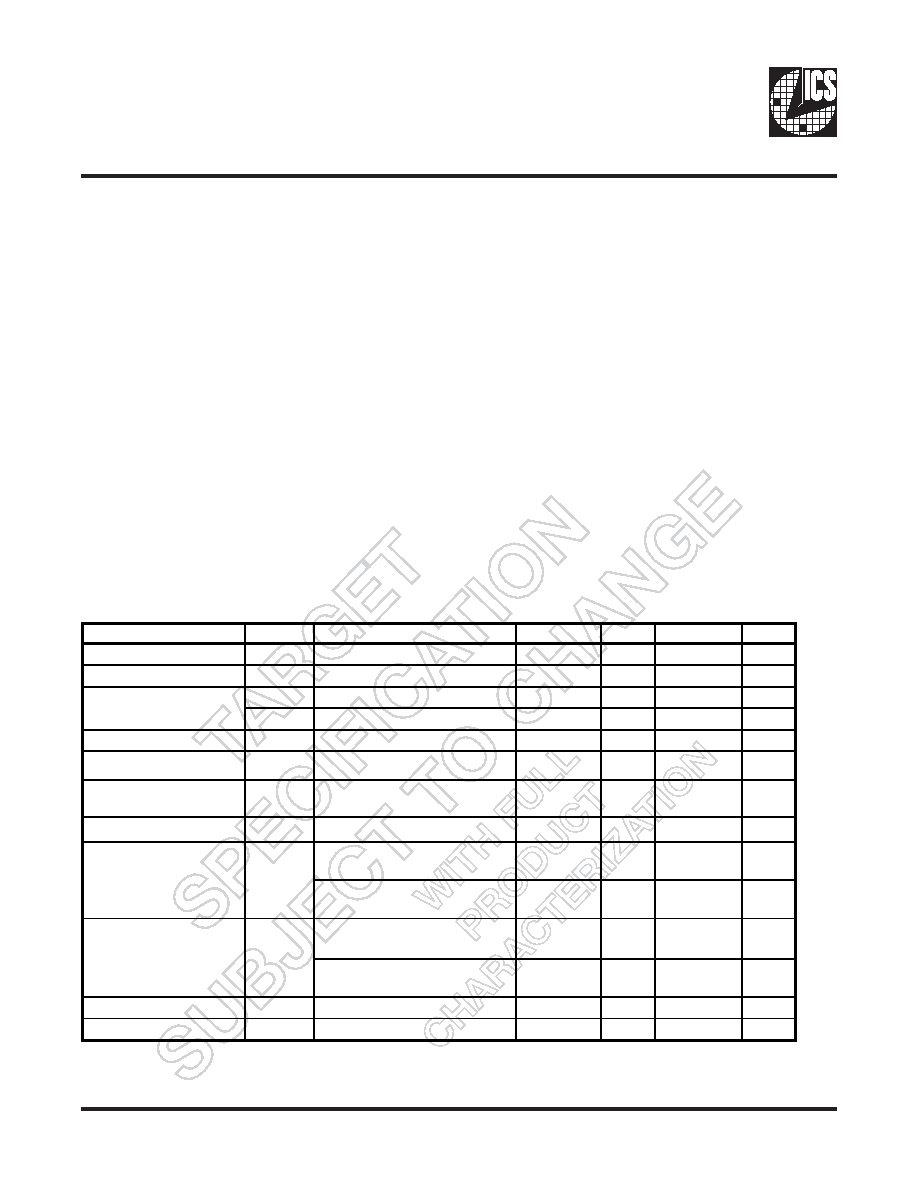
Electrical Characteristics - Input/Supply/Common Output Parameters
TA = 0 - 85°C; Supply Voltage AVDD, VDD = 2.5 V +/- 0.2V (unless otherwise stated)
PARAMETER
SYMBOL
CONDITIONS
MIN
TYP
MAX
UNITS
Input High Current
IIH
VI = VDD or GND
A
Input Low Current
IIL
VI = VDD or GND
A
IDD2.5
CL = 0pf
mA
IDDPD
CL = 0pf
100
mA
Output High Current
IOH
VDD = 2.3V, VOUT = 1V
-18
mA
Output Low Current
IOL
VDD = 2.3V, VOUT = 1.2V
26
mA
High Impedance
Output Current
IOZ
VDD=2.7V, Vout=VDD or
GND
±10
mA
Input Clamp Voltage
VIK
Iin = -18mA
V
VDD = min to max,
IOH = -1 mA
V
VDD = 2.3V,
IOH = -12 mA
V
VDD = min to max
IOL=1 mA
0.1
VDD = 2.3V
IOH=12 mA
0.6
V
Input Capacitance
1
CIN
VI = GND or VDD
pF
Output Capacitance
1
COUT
VOUT = GND or VDD
3
pF
1Guaranteed by design, not 100% tested in production.
Operating Supply
Current
High-level output
voltage
VOH
Low-level output voltage
VOL
相关PDF资料 |
PDF描述 |
|---|---|
| 93V855AGLFT | 93V SERIES, PLL BASED CLOCK DRIVER, 5 TRUE OUTPUT(S), 0 INVERTED OUTPUT(S), PDSO28 |
| 93V855AGLF | 93V SERIES, PLL BASED CLOCK DRIVER, 5 TRUE OUTPUT(S), 0 INVERTED OUTPUT(S), PDSO28 |
| 93V855AG | 93V SERIES, PLL BASED CLOCK DRIVER, 5 TRUE OUTPUT(S), 0 INVERTED OUTPUT(S), PDSO28 |
| 93V855AGI | 93V SERIES, PLL BASED CLOCK DRIVER, 5 TRUE OUTPUT(S), 0 INVERTED OUTPUT(S), PDSO28 |
| 93V857BG-025LF-T | 93V SERIES, PLL BASED CLOCK DRIVER, 10 TRUE OUTPUT(S), 0 INVERTED OUTPUT(S), PDSO48 |
相关代理商/技术参数 |
参数描述 |
|---|---|
| 93V855AGI | 功能描述:时钟驱动器及分配 RoHS:否 制造商:Micrel 乘法/除法因子:1:4 输出类型:Differential 最大输出频率:4.2 GHz 电源电压-最大: 电源电压-最小:5 V 最大工作温度:+ 85 C 封装 / 箱体:SOIC-8 封装:Reel |
| 93V855AGIT | 制造商:Integrated Device Technology Inc 功能描述:34-LANE, 16-PORT PCIE GEN2 SYSTEM INTERCONNECT SWITCH 制造商:Integrated Device Technology Inc 功能描述:28 TSSOP - Tape and Reel |
| 93V855AGLF | 功能描述:时钟驱动器及分配 RoHS:否 制造商:Micrel 乘法/除法因子:1:4 输出类型:Differential 最大输出频率:4.2 GHz 电源电压-最大: 电源电压-最小:5 V 最大工作温度:+ 85 C 封装 / 箱体:SOIC-8 封装:Reel |
| 93V855AGLFT | 功能描述:时钟驱动器及分配 RoHS:否 制造商:Micrel 乘法/除法因子:1:4 输出类型:Differential 最大输出频率:4.2 GHz 电源电压-最大: 电源电压-最小:5 V 最大工作温度:+ 85 C 封装 / 箱体:SOIC-8 封装:Reel |
| 93V857BG-025LF | 功能描述:时钟驱动器及分配 RoHS:否 制造商:Micrel 乘法/除法因子:1:4 输出类型:Differential 最大输出频率:4.2 GHz 电源电压-最大: 电源电压-最小:5 V 最大工作温度:+ 85 C 封装 / 箱体:SOIC-8 封装:Reel |
发布紧急采购,3分钟左右您将得到回复。